Using High Frequency PCBs
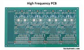
High frequency pcbs are essential for electronic devices that require high-speed digital signals. Their ability to regulate impedance for fast data transmission and reduce insertion loss improves signal integrity and performance. However, they are also vulnerable to noise and distortion. It is therefore necessary to choose the best PCB for your needs.
The key to successful high-frequency PCB manufacturing lies in the material used for its construction. Conventional FR-4 substrates have limited performance in high-frequency applications because of their increased dielectric losses and dispersion. Instead, specialized materials such as Rogers and Teflon are preferred for high-frequency PCB design. These materials have lower dielectric losses and a stable loss tangent over the entire frequency spectrum.
In addition to the selection of the appropriate materials, the thickness of a high-frequency PCB plays an important role in its performance. Thicker boards have greater thermal stability, which helps reduce temperature fluctuations and jitter. In turn, this improves circuit performance and increases reliability. In addition, thicker boards have better thermal conductivity, which allows for efficient heat transfer between copper foils.
Another crucial factor in achieving high-frequency performance is the choice of the copper material and its surface finish. Ideally, the copper should have low skin effect losses and be available in a range of sizes. Moreover, the copper should be plated using an electroless nickel or immersion gold process to minimize losses and maximize its performance.
Advantages of Using High Frequency PCBs
Other factors that can influence a high frequency pcb performance include the design of power and ground planes, routing of signals, and shrinking the size of pads to minimize parasitic capacitance. During the PCB design process, designers must take into account all of these factors to ensure that their finished products will be reliable.
The design of a high-frequency PCB is complex and requires careful planning. Unlike ordinary electronic circuits, HF PCBs have a higher impedance tolerance and a larger bandwidth. They can be used in a variety of applications, including avionics systems, radar sensors, and missile guidance equipment. High-frequency PCBs are also ideal for medical devices such as magnetic resonance imaging (MRI) and computed tomography (CT) scanning.
When designing a high-frequency circuit board, it is essential to use a multi-layer design to maintain optimum performance. The layers should be separated by airspace to avoid interference between signals. It is also recommended to use a large ground plane and a narrow trace width to reduce coupling between the signal and power lines.
The first step in designing a high-frequency circuit board is to select the proper laminate material. Look for a material with a low loss tangent and good thermal stability. Then, decide whether to use a solid or a hybrid design. Finally, determine the number of layers and the order in which they are stacked. Ideally, you should use a low-cost material for the outermost layer and higher-speed material for inner layers. This way, you can minimize cost without sacrificing the performance of your final product. Additionally, it is critical to plan the layout of the components and traces on a checklist before starting the assembly process.